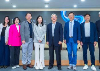
On 16 June 2025, the Taiwan–UK Sustainability Research and Development Forum was held at the Entopia Building, home to the Cambridge Institute for Sustainability Leadership (CISL) at the University of Cambridge. Co-hosted by Taiwan’s National Institutes of Applied Research (NIAR) and CISL, the forum aimed to strengthen collaboration between Europe and Asia across scientific research, industry and sustainability governance.
The discussions centred on critical themes including advanced materials, low-carbon technologies, energy infrastructure and next-generation semiconductor manufacturing. Leading research institutions and industry figures from across Europe and Asia gathered to exchange insight and explore new models of cooperation.
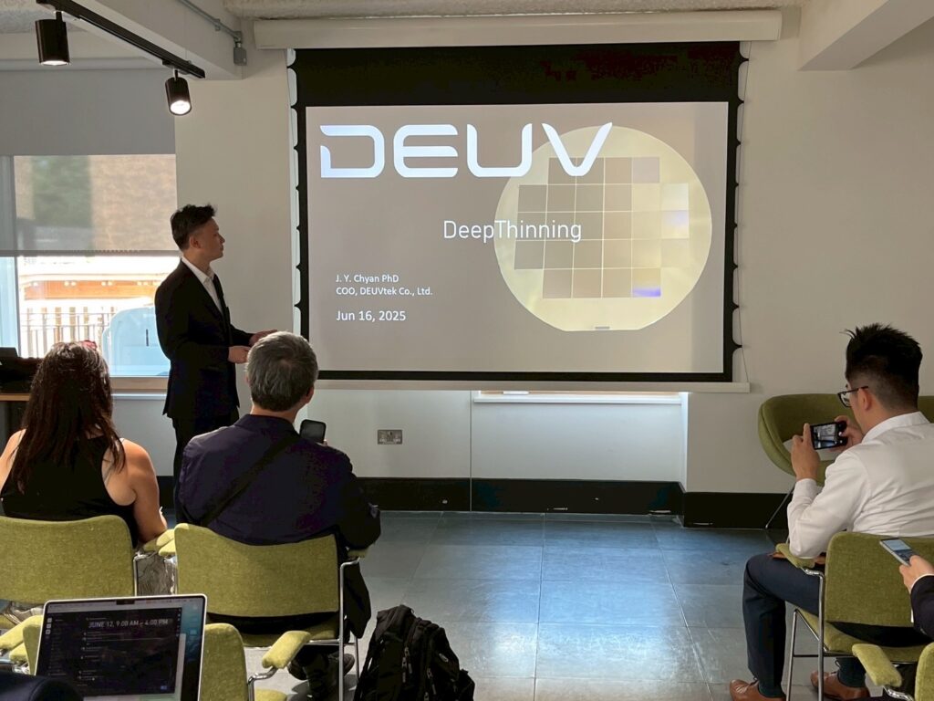
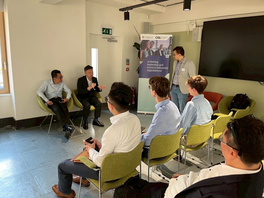
During the forum, Dr. Jiunn-Yih Chyan, Chief Operating Officer of DEUVtek, was invited to deliver a keynote address. He shared perspectives on the silicon carbide materials revolution, sustainable manufacturing and the future trajectory of advanced packaging technologies. His insights drew significant interest from European research bodies and global industry stakeholders.
As the forum’s media strategy partner, the London editorial team of the British publication The Icons conducted an in-depth interview with Dr. Chyan at the Entopia Building, capturing his views on the global semiconductor ecosystem, sustainable production models and the innovation pathways shaping the industry’s future.
The Turning Point in Materials Technology: From Industry Pain Points to Innovation Momentum
When discussing the founding vision of DEUVtek, Dr. Chyan did not shy away from the realities of the industry. Instead, he addressed the core issues with a distinctly strategic perspective. He noted that the rapid expansion of AI, electric vehicles, 5G and low-Earth-orbit satellites has pushed global expectations for semiconductor materials and energy efficiency into a new era.
Traditional silicon is no longer sufficient for the demands of emerging technologies. While silicon carbide (SiC) and gallium nitride (GaN) offer significant performance advantages as next-generation compound semiconductors, their extreme hardness, corrosion resistance and processing challenges have created structural bottlenecks for the industry—particularly in achieving mass production and reliable yield rates.
In the interview, Dr. Chyan outlined this technological inflection point with clarity: “Breakthroughs in materials do not automatically translate into value. If manufacturing processes cannot keep pace, material revolutions will never truly enter the industry.” His analysis reflects a growing consensus across the semiconductor sector: the next decade of competition will hinge not only on material innovation but also on whether manufacturing processes can accommodate new materials and build a stable supply chain.
“DEUVtek was established on the basis of these industry realities,” he emphasised. “What I want to highlight is that companies must begin with the structural pain points of the value chain and grasp the challenges shared across global markets. Only then can they define their position in the next wave of technological evolution.”
DeepThinning: A Technical Breakthrough Reshaping Silicon Carbide Manufacturing
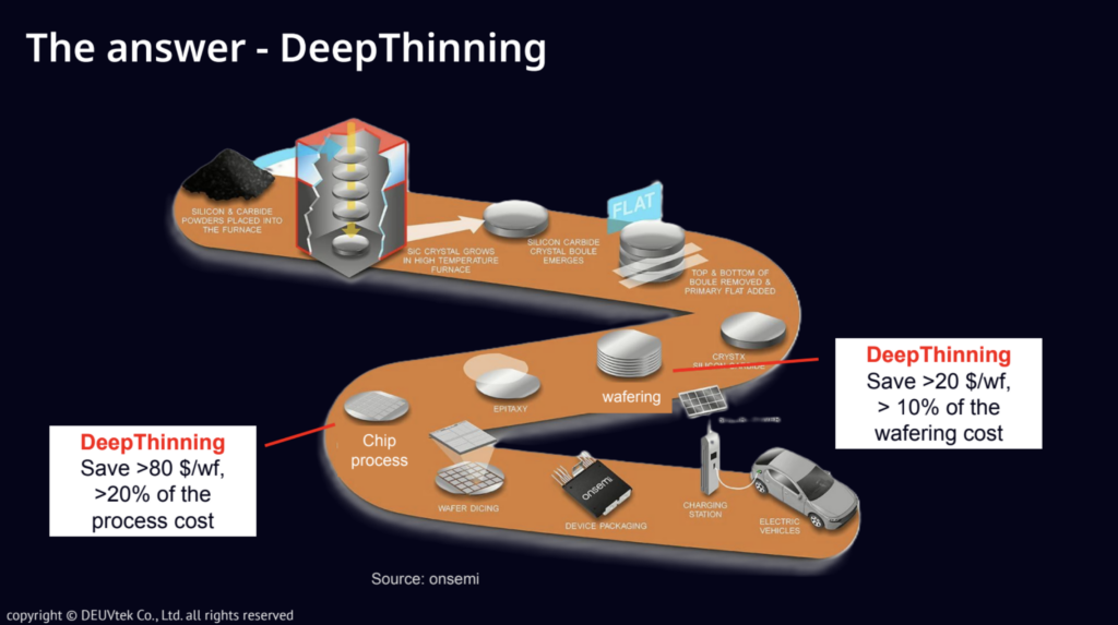
When discussing DEUVtek’s core DeepThinning technology, Dr. Chyan spoke with the precision of a scientist, outlining both its technical significance and its broader industrial implications. He explained that while silicon carbide offers unparalleled advantages in energy conversion efficiency, voltage resistance and thermal conductivity, its extreme hardness and corrosion resistance have made traditional machining methods—such as mechanical grinding and gas etching—reach their limits in efficiency, yield and consumable costs.
DeepThinning replaces these consumable-intensive processes with an innovative optical-laser mechanism that enables entirely non-contact manufacturing. This dramatically reduces wafer breakage and significantly increases processing speed. “When a process no longer relies on mechanical force, the issues of material stress and wafer breakage can be solved at their root,” Dr. Chyan noted. “This is not just an improvement in efficiency; it is a fundamental redefinition of the logic behind silicon carbide processing.”
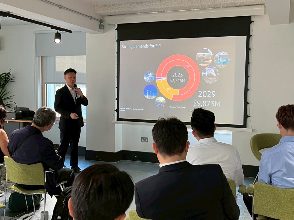
In measurable results, DeepThinning has reduced breakage rates from the industry norm of around 3 percent to below 0.1 percent, enabling stable mass production of ultra-thin wafers below 50 micrometres. With consumables essentially eliminated, overall manufacturing costs fall by roughly 20 percent. The process also removes diamond grinding wheels, oil-water cleaning and consumable waste streams—major sources of carbon emissions—ushering silicon carbide production into a genuinely sustainable model.
According to Dr. Chyan, the technology has attracted significant attention from research groups at Cambridge precisely because it delivers three forms of high-level global impact: a restructured cost model, enhanced industrial scalability and a practical pathway for embedding sustainability into next-generation semiconductor manufacturing.
The Taiwanese Model of Sustainable Manufacturing: Systemic Resilience Built Within Constraints
When speaking about sustainable manufacturing, Dr. Chyan analysed Taiwan’s position through a broad structural lens. He pointed out that Taiwan is not only a global centre for advanced semiconductor manufacturing, but also one of the first regions to confront the constraints of limited water, electricity and land resources, alongside intensifying international pressure on carbon emissions. The fact that Taiwan continues to maintain the world’s highest yield rates and the most complete supply chain under these conditions reflects what he describes as a form of “systemic resilience”: the ability to keep innovating despite multiple constraints.
During the interview, he emphasised: “Taiwan’s strategic importance does not rest solely on technological leadership, but on its ability to practise sustainable manufacturing under resource pressure.” This form of sustainability is not an optional add-on, but an embedded element of Taiwan’s entire production logic.
Dr. Chyan explained that DeepThinning fits squarely within this context. By reducing carbon emissions, eliminating consumables and improving production stability, the technology becomes a key component of Taiwan’s strategy for a sustainable global supply chain. It enables silicon carbide manufacturing to achieve both environmental benefit and industrial competitiveness—an advantage that will shape Taiwan’s role in the next generation of semiconductor development.
International Expansion: Europe as the First Proving Ground for Technology and Policy
When asked why Europe was chosen as the starting point for DEUVtek’s international expansion, Dr. Chyan offered a clear, strategy-driven explanation. Europe, he noted, is simultaneously the global architect of sustainability regulations, a major centre for compound-semiconductor research and the region with the most ambitious energy-transition policies. Just as crucial is the continent’s shift toward a “local for local” production model in response to geopolitical tensions and a fragmented supply chain. Under this model, companies that can demonstrate sustainable processes, high reliability and the ability to build localised operations gain trust and market access far more rapidly.
He also highlighted the pivotal role of the National Institutes of Applied Research (NIAR): “NIAR provides the practical mechanisms that connect Taiwan directly with Europe’s research institutions, policy networks and technological ecosystem.”
Through instrument-sharing frameworks, cross-disciplinary projects, international research agreements and overseas research hubs such as the ACDRC (Advanced Chip Design Research Center, established by Taiwan’s Ministry of Foreign Affairs and the Czech Republic), Taiwanese companies can integrate swiftly into Europe’s technology system and validate their innovations under some of the world’s strictest standards.
According to Dr. Chyan, this approach is not only about expanding markets; it is, more fundamentally, about gaining “access to the arena of international technology governance.”
Becoming a Driving Force in the Global Reconfiguration of the Semiconductor Supply Chain, Not Just an Equipment Provider
Looking ahead, Dr. Chyan observed that the global semiconductor industry is shifting from a “process-scaling race” to a “system-performance race”. Heterogeneous integration, 2.5D and 3D packaging and the rise of chiplet architectures will define the next phase of industry development, and Taiwan sits firmly at the centre of this transition. With its dense technical capability and fully developed ecosystem in advanced packaging, Taiwan is uniquely positioned to shape the global chiplet landscape.
Against this backdrop, DEUVtek’s role is becoming increasingly distinct: to serve as a pivotal equipment provider in advanced packaging and new-material manufacturing, while using its R&D base in Taiwan to establish trusted technological footholds across Europe and the United States.
“Our aim is not to chase scale, but to become the most reliable technological partner amid the uncertainties of the global supply chain,” Dr. Chyan emphasised. “This strategic model will enable DEUVtek to act as a system-level force in the reconfiguration of the global semiconductor supply chain, rather than merely a supplier of individual equipment.”
Recommend for you:
Euro–Asia Collaboration on Sustainability: Redefining the Global Order


